Documentation
For a detailed description of the theoretical aspects see Related Publications.Input Signal
In the current implementation each individual modulator is optimized via single sine wave inputs at eight different amplitudes but with the same input frequency. These amplitudes are linearly spaced between selectable minimum and maximum values \(A_\mathrm{min}\) and \(A_\mathrm{max}\). The frequency can be set in percent of the inband.
Amplitude
The eight input amplitudes of the signals are defined in a range between \(A_\mathrm{min} = [0.001;A_\mathrm{max})\) and \(A_\mathrm{max} = (A_\mathrm{min};2]\). For the final optimized result, a complete amplitude sweep is performed in order to show the complete dynamic range performance.
-
Hints for the optimization:
The covered range of the amplitudes can be utilized in order to aim for a certain maximum stable amplitude (MSA). E.g., when selecting 0.7 for \(A_\mathrm{min}\) and 0.8 for \(A_\mathrm{max}\), only modulators which are stable in that range are evaluated as good. However, the tougher the constraints the higher the chance that no modulator can be found at all.
-
Examples:
Selecting for the minimum and maximum amplitude values:
- \(A_\mathrm{min} = 0.3\)
- \(A_\mathrm{max} = 1.0\)
results in the test amplitudes:
Test signal # 1 2 3 4 5 6 7 8 Test amplitude 0.3 0.4 0.5 0.6 0.7 0.8 0.9 1.0
Frequency
The normalized input frequency \(f_\mathrm{norm}\) can be set between \([0.01;1]\) in \(\frac{f}{f_\mathrm{s}}\).
-
Hints for the optimization:
Inserting a frequency lower than \(\frac{1}{3}\) times the inband will include the third harmonic produced by the quantizer. Thereby, the more robust modulators are favoured.
-
Examples:
Selecting a frequency of
- \(f_\mathrm{norm} = 0.3\)
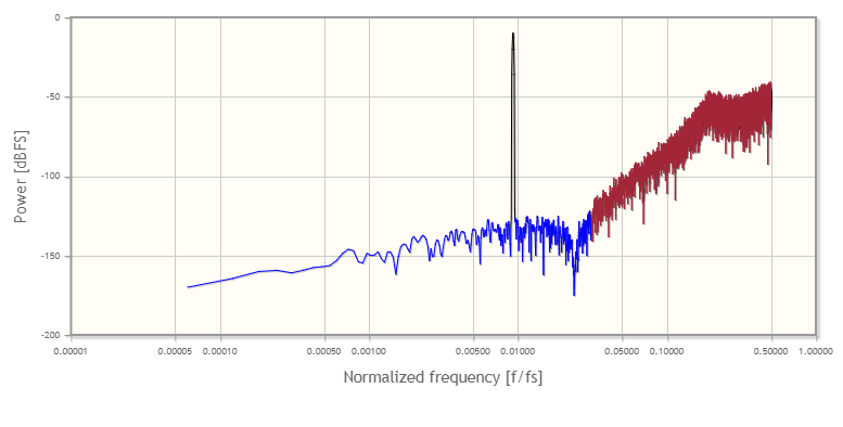
results in a tone right in the middle of the band of interest at \(0.3\cdot\frac{f_\mathrm{s}}{2\cdot\mathrm{OSR}}\). Increasing or decreasing the value shifts the signal peak indicated by the arrows in the following figure.
Integrators/Resonators
The current implementation allows selecting one out of seven CT integrator and resonator types, each of them providing their individuel set of parameters. Depending on the chosen type, the tool offers different design goals and constraints. Moreover, the selection affects the available settings in the D/A converter and coefficient blocks.
For DT modulators, an ideal integrator is available.
| Model Type | Integrator/Resonator model type. |
| Dynamics | Optimize for a defined minimum and maximum integrator/resonator output swing. |
| DC gain | DC Gain of the integrator/resonator.. |
| GBW/Bandwidth | Represents the GBW or location of the first pole depeding on the model type. |
| Resonance Frequency | Resonance Frequency if supported by the model. |
| Prop. path | High-level coefficient representing a proportional path, if supported by the model. |
Model type
DT Integrators
Ideal
Ideal integrator means, the integrator is ideal by all matters.
CT Integrators
Ideal
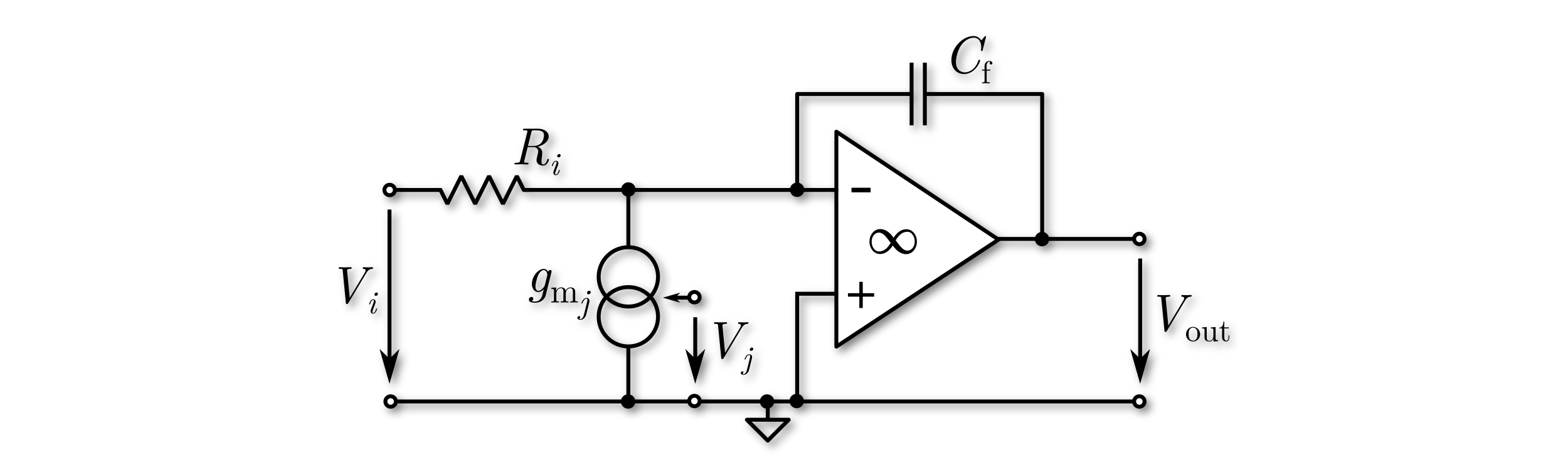
Ideal integrator means, the integrator is ideal by all matters. There are no limitations in DC gain, GWB, etc. Each ideal integrator represents one state in the state-space model of the overal modulator model, which is used for optimization. A circuit-level model is shown in the figure below. Here, the circuit-level model utilizes an ideal OpAmp with a transfer characteristic of \(A(s)= \infty\). Feedback paths of the modulator are represented by the ideal current source with \(V_j\) as input.
OpAmp Integrator
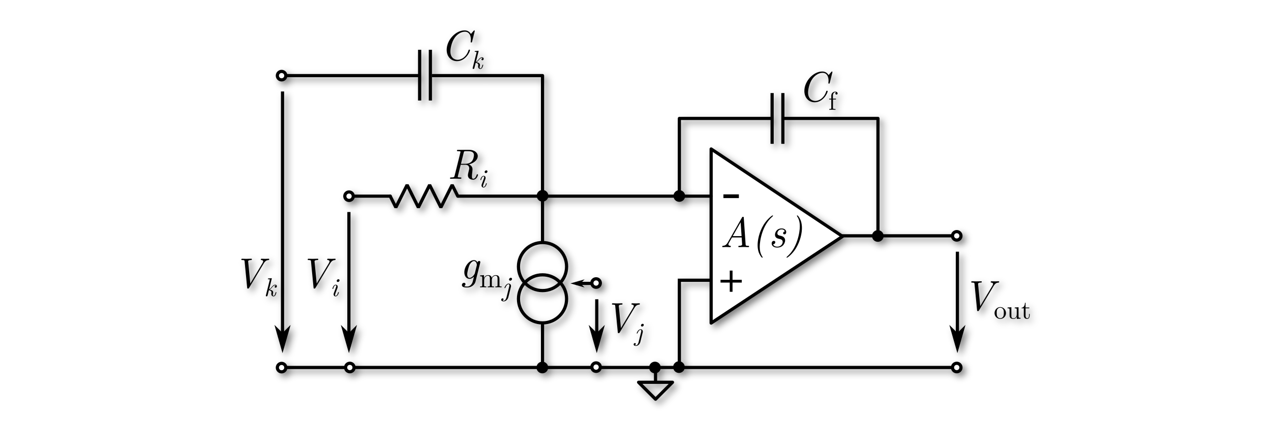
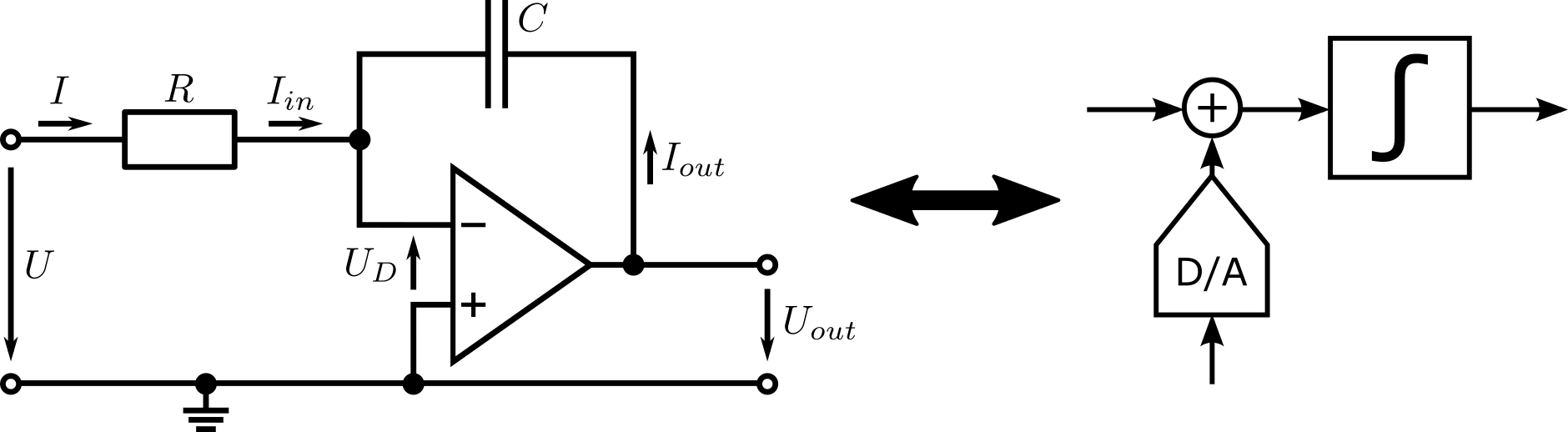
In the OpAmp based integrator model, the dominant pole of the OpAmp is accounted for in order to investigate the most dominant non-ideal behavior. By this pole, finite DC gain and finite GBW can be modeled. Each OpAmp based integrator represents two states in the state-space model of the overal modulator model, which is used for optimization, obviously leading to smaller simulation throughputs than the ideal models. The model supports resistive and capacitive inputs represented by \(V_i\) and \(V_k\) in the circuit-level diagram below. Feedback paths of the modulator are represented by the ideal current source with \(V_j\) as input. During the optimization gain errors due to multiple resistive inputs are accounted for automatically.
OpAmp Integrator with Proportional Path
As in the OpAmp based integrator model without proportional path, the dominant pole of the OpAmp is accounted for in order to investigate the most dominant non-ideal behavior. By this pole, finite DC gain and finite GBW can be modeled. Also each OpAmp based integrator with proportional path represents two states in the state-space model of the overal modulator model, which is used for optimization, obviously leading to smaller simulation throughputs than the ideal models. The proportional path is formed by the risistor \(R_p\). During the optimization gain errors due to multiple resistive inputs are accounted for automatically. The model is implemented as shown below in the circuit-diagram. Therefore, possible resonators feed back not only the integrated but also the proportionally scaled signal. The model supports resistive inputs represented by \(V_i\) in the circuit-level diagram below. Feedback paths of the modulator are represented by the ideal current source with \(V_j\) as input.

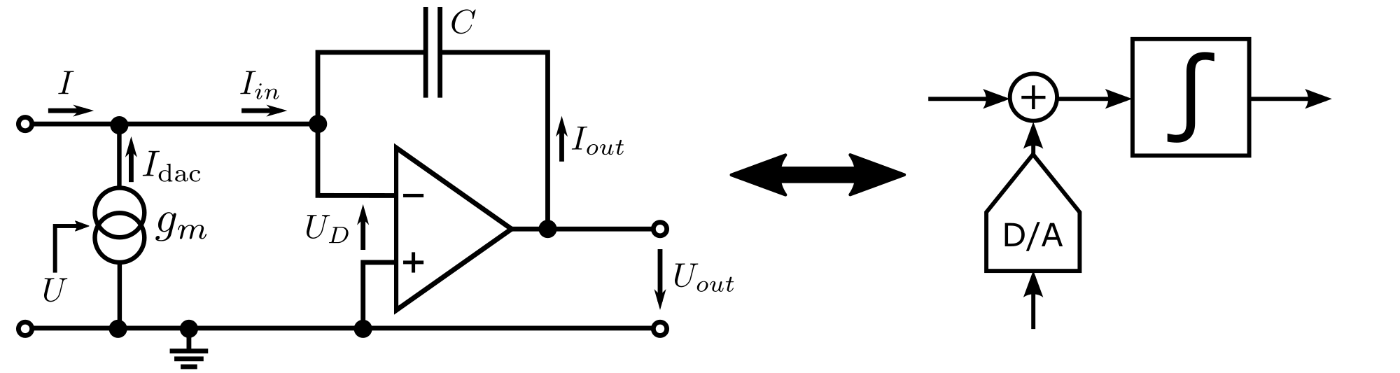
gm-C Integrator
As an alternative, an OTA based integrator model is available. Each input path is formed by its own OTA with input voltage \(V_i\) and the frequency dependant gain \(g_\mathrm{m}(s)\), which shows one-pole behaviour. The pole location specifies the bandwidth of the OTA. A finite output transconductance is accounted by \(g_\mathrm{out}\). The model is implemented as shown below in the circuit-diagram. The model is represented in the state-space model of the overal modulator model by two states.

CT Resonators
Ideal
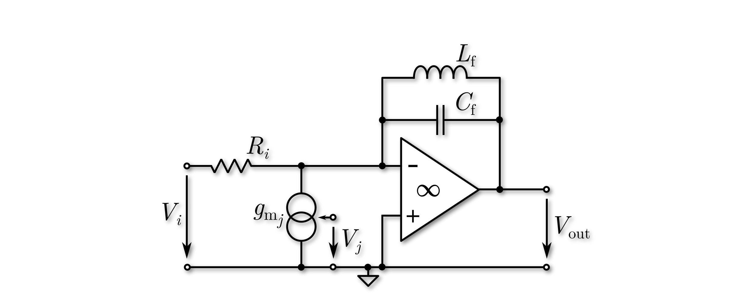
Ideal resonator means, the resonator is ideal by all matters. There are no limitations in DC gain, GWB, Q, etc. Each ideal resonator represents two states in the state-space model of the overal modulator model, which is used for optimization. A circuit-level model is shown in the figure below incorporating an LC resonator. Here, the circuit-level model utilizes an ideal OpAmp with a transfer characteristic of \(A(s)= \infty\). Feedback paths of the modulator are represented by the ideal current source with \(V_j\) as input.
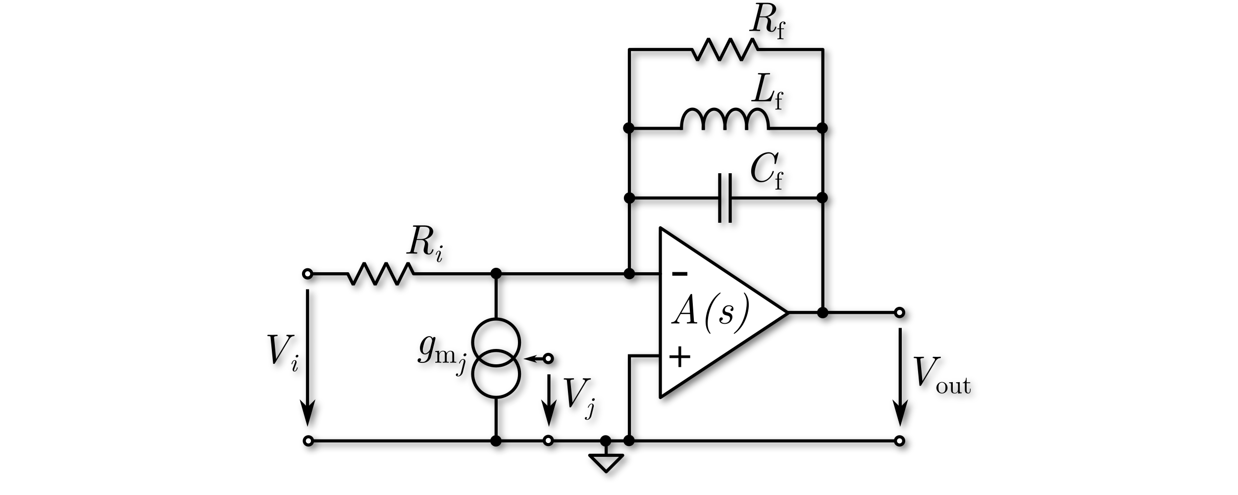
OpAmp LC Resonator
In the OpAmp based resonator model, the dominant pole of the OpAmp is accounted for in order to investigate the most dominant non-ideal behavior. By this pole, finite DC gain and finite GBW can be modeled. Each OpAmp based resonator represents three states in the state-space model of the overal modulator model, which is used for optimization, obviously leading to smaller simulation throughputs than the ideal models. The model supports resistive inputs represented by \(V_i\) in the circuit-level diagram below. Feedback paths of the modulator are represented by the ideal current source with \(V_j\) as input. The finite resistance \(R_f\) is used to model a finite quality factor Q.
gm-LC Resonator
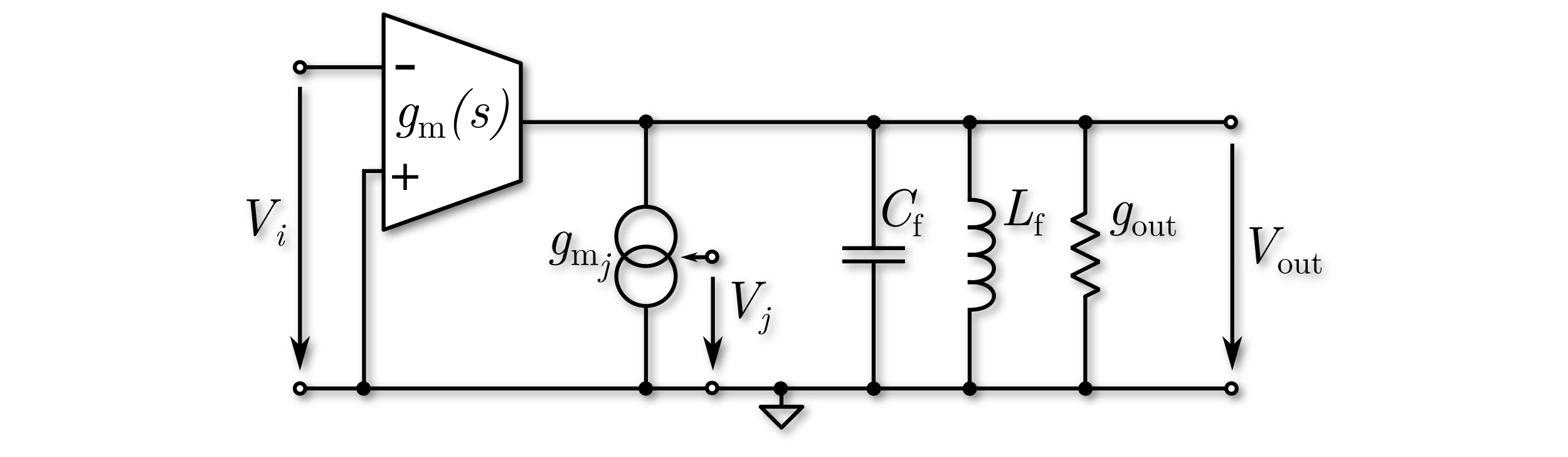
An OTA based resonator model is also available. Each input path is formed by its own OTA with input voltage \(V_i\) and the frequency dependant gain \(g_\mathrm{m}(s)\), which shows one-pole behaviour. The pole location specifies the bandwidth of the OTA. The output transconductance is \(g_\mathrm{out}\) used to model a finite quality factor Q. The model is implemented as shown below in the circuit-diagram. The model is represented in the state-space model of the overal modulator model by three states.
Dynamics
For each of the integrator and resonator models, an optimization goal for the output swing \(V_\mathrm{out}\) can be set. Modulators with swings lower than the \(V_\mathrm{out,min}\) or higher then the \(V_\mathrm{out,max}\) value are rated worse than ones within this boundaries.
DC gain
For non-ideal OpAmp based model, a DC gain parameter \(A_\mathrm{DC}\) can be set. It can be minimized or a fixed value can be set.-
Minimize:
Allows the genetic algorithm to change the DC gain in order to find a minimal acceptable value. This option enables the choice of \(A_\mathrm{DC,min}\) and \(A_\mathrm{DC,max}\) boundaries for a defined, allowed range.
-
Fixed:
Fixes the DC gain to a defined value during optimization. This option enables to choose the defined value in the range \(A_\mathrm{DC} \in [10;100000]\) on an absolute scale.
-
Hints for Optimization:
Low DC gain values will result in poor linearity, which is not investigated during the optimization!
GBW/Bandwidth
Depending on the type of the non-ideal models, GBW or bandwidth are available as parameters. For OpAmp based models, GBW is used, for OTA based models bandwidth. Both \(f_\mathrm{gbw},f_\mathrm{b} \in [0.01;10]\) are normalized to \(f_\mathrm{s}\). Higher values than 10 times \(f_\mathrm{s}\) are considered as ideal and, thus, not supported. Both can be minimized or a fixed value can be set.
-
Minimize:
Allow the genetic algorithm to change \(f_\mathrm{gbw}/f_\mathrm{b}\) in order to find a minimal acceptable value. This option enables the choice of \(f_\mathrm{min}\) and \(f_\mathrm{max}\) boundaries for an allowed range.
-
Fixed:
Fixes \(f_\mathrm{gbw}/f_\mathrm{b}\) to a defined value during optimization.
Resonance Frequency
For resonator models, the resonance frequency parameter \(f_0\) is shown. It is connected to the design goal that tries to place this frequency in the inband of the modulator. \(f_0\) is normalized to \(f_\mathrm{s}\).
-
Optimize:
Allow the genetic algorithm to change \(f_0\) in order to find an optimal value. This option enables the choice of \(f_\mathrm{min}\) and \(f_\mathrm{max}\) boundaries for an allowed range.
-
Fixed:
Fixes \(f_0\) to a defined value during optimization.
Proportional Path
This parameter is only available for the model type OpAmp Integrator with Proportional Path. Possible options are:-
Optimize:
Optimize enables the genetic algorithm to change the value of this coefficient in order to find a better modulator. This option enables the choice of \(k_\mathrm{min}\) and \(k_\mathrm{max}\) boundaries for a defined, allowed range.
-
Fixed:
Fixes the coefficient \(k \in [0.00001;10)\) to a defined value during optimization.
High-Level Coefficients
In the high-level block diagram the modulator coefficients are ideal signal scaling blocks. Nevertheless, in order to account also for low-level behavior, some additional options are implemented if certain integrator or resonator models are selected. E.g., if the OpAmp Integrator model is selected, the designer can choose between resistive or capacitive coupling of the feed forward paths targeting that integrator, which effects the output swings and the integrator gain error.
For the optimization all coefficients of the modulator can be individualized seperately. The designer can set fixed coefficient values or optimize the values with or without previously set upper and lower boundaries as optimization goals.
| Activate/Deactivate | Enable/disable path during optimization. |
| Type | Path realization via resistor. |
| Value | Optimize coefficient value. |
Activate/Deactivate
This option adds or removes the coefficient from the block diagram. It is available for all coefficients but \(b_1\), since this is considered as mandatory.
Coupling Type
If the OpAmp Integrator model is selected, there are two options for the coupling of the coefficient with the integrator. For all other models, the respective modelled coupling type is used.
-
Resistive:
Resistive input means the input to the integrator is formed by a resistor as shown below. This path affects the integrator gain, which is accounted for automatically.
-
Capacitive:
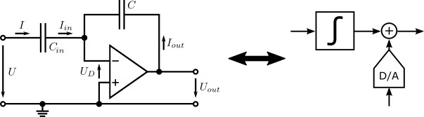
Capacitive input means the input to the integrator is formed by a capacitor as shown below. In this case, a high-level path according to the model in the main window is formed across an integrator even though in the low-level domain the signal is forwarded by the proportional behavior through the integrator. This path does not affect the integrator gain but certainly the integrator swing. Capacitive paths with ideal models can be investigated by inserting appropriate ideal paths.
Coefficient Value
The coefficient value is the main parameter of this block. It represents the high-level coefficient itself. It can be either fixed to a certain value or optimized.
-
Optimize:
This option enables the genetic algorithm to change the value of this coefficient in order to find a better modulator. This option enables the choice of minimum and maximum boundaries for a defined range, which is allowed for the coefficient.
-
Fixed:
It is possible to set the coefficient to a defined value during optimization. Possible values are: \(b_x,c_x,d_x,e_x \in [0.00001;10)\).
-
Same as \(a_1\):
Fix the coefficient \(b_1\) to the same value as \(a_1\) during optimization. This option is set by default for lowpass modulators. Modulators, which do not have any other inputs to the first summing node than the paths through \(a_1\) and \(b_1\), exhibit an STF of 0 dBFS for low frequencies, if \(b_1\) equals \(a_1\).
Internal Quantizer
The quantizer is considered as an ideal element, while dithering is possible.
| Quantizer levels | Number of quantizer levels |
| Dithering | Add random noise onto the quantizer input |
| Dynamics | Optimize for a defined quantizer input swing |
Quantizer Levels
This parameter defines the number of levels \(N_\mathrm{levels} \in [2;64]\) in the quantizer. An even number results in a mid-rise, while an odd number results in a mid-thread quantizer characteristic.
Dithering
This option adds noise onto the quantizer input during each sampling instant. The noise is uniformly distributed and the interval is defined by +/- the chosen value. Possible values for dithering are in the rage of \([0;1]\), while the value is normalized to one quantizer stepwidth and thus scales down automatically with increasing number of quantizer levels.
Dynamics
For the quantizer, an optimization goal for the input swing \(V_\mathrm{in}\) can be set. Modulators with swings lower than the \(V_\mathrm{in,min}\) or higher then the \(V_\mathrm{in,max}\) value are rated worse than ones within this boundaries.
D/A Converter
The D/A converters (DACs) of the block diagram form the feedback paths and can account for some low-level behavior. Different input coupling options are available if certain integrator or resonator models are selected. E.g., if the OpAmp Integrator model is selected, the designer can choose in between resistive or current source coupling, which effects the output swings and the integrator gain error and, moreover, the last feedback DAC can be coupled capacitivly.
For the optimization all DACs of the modulator can be individualized seperately. The designer can set fixed coefficient values or optimize the values with or without previously set upper and lower boundaries as optimization goals. Further, the output waveform and a local delay can be set.
| Activate/Deactivate | Enable/disable path during optimization. |
| Type | Path realization via resistor. |
| Value | Optimize coefficient value. |
| D/A settings | Local delay of the signal |
Activate/Deactivate
This option adds or removes the DAC from the block diagram. It is available for all DACs but \(a_1\), since these are considered as mandatory.
Type
There are up to three options for the coupling of the DAC with the integrator or resonator, depending on the selected model. The last DAC has more options, as its signal is added to the output of the last integrator.
-
Resistive:
Resistive input means the input is formed by a resistor as seen below. This path affects the integrator gain, which is accounted for automatically. OpAmp based non-ideal integrators allow this option.
-
Capacitive:
Capacitive input is only available for the last DAC in combination with the non-ideal OpAmp Integrator model. It means that the path is formed by a capacitor to the last integrator as seen below. In the block diagram this path is represented by a summation of the signals after the integrator. In this case, a high-level path according to the model in the main window is formed across an integrator even though in the low-level domain the signal is forwarded by the proportional behavior through the integrator. This path does not affect the integrator gain but certainly the integrator swing. The capacitive path with the ideal model can be investigated by inserting the appropriate ideal path.
-
Current Source:
Current source means the input is formed by a current source. The integrator/resonator gain is not affected.
Coefficient Value
The DAC coefficient value is the main parameter of this block. It represents the high-level coefficient itself. It can be either fixed to a certain value or optimized.
-
Optimize:
This option enables the genetic algorithm to change the value of this coefficient in order to find a better modulator. This option enables the choice of minimum and maximum boundaries for a defined range, which is allowed for the coefficient.
-
Fixed:
It is possible to set the coefficient to a defined value during optimization. Possible values are: \(a_x \in [0.00001;10)\).
D/A settings
-
Local ELD:
The value for the local excess-loop-delay can be chosen to ELD \(\in [0;1]\). In contrast to the global ELD it is an individual value for each DAC. The summation of global and local ELD has to be in the range \([0;1]\). Here, the value is normalized to the duration of one sampling clock cycle \(T_\mathrm{s} = \frac{1}{f_\mathrm{s}}\).
-
Waveform:
The DAC output waveform can be chosen individually for each feedback DAC. Non-return-to-zero (NRZ), return-to-zero (RZ), raised cosine (RCOS) and exponential decay (EXP) are available.
Global Excess-Loop-Delay
The Global Excess-Loop-Delay block adds an global ELD to all feedback paths.
| Excess-loop-delay | Combined delay of the quantizer and DAC. |
Excess-loop-delay
The value for the ELD can be chosen to ELD \(\in [0;1]\). The summation of global and local ELD has to be in the range \([0;1]\). Here, the value is normalized to the duration of one sampling clock cycle \(T_\mathrm{s} = \frac{1}{f_\mathrm{s}}\).